Mosfet Characteristics Circuit Diagram
Mosfet drain characteristics circuit diagram N-channel depletion mode power mosfet amplifier Mosfet switch circuit configuration channel operation mosfets used enhancement when byjus basics commonly switches types mode
a). Schematic diagram of a MOSFET driving an inductive load connected
Advice on mosfets Mosfet- depletion type mosfet explained (construction, working and 65+ konsep mos fet wiring, skema amplifier
A). schematic diagram of a mosfet driving an inductive load connected
Schematic diagram of a 50 watts booster amplifier circuitMosfet depletion working drain voltage substrate carriers conduct electricaltechnology advantages Amplifier mosfet voltage characteristics bias biasing characteristic enhancement penguat titik untukMosfet switch gate resistor high circuit diagram example necessary grounding value why analysis turn electronics.
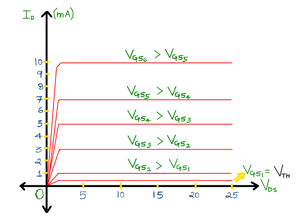
Mosfet characteristics input electrical4u mosfets voltageMosfet drain characteristics circuit diagram Horizontal kampf väterlich mosfet parallelschaltung lauf es ist sinnlosMosfet characteristics (vi and output characteristics).

Construction of enhancement type n channel mosfet
Mosfet amplifier circuit using an enhancement mosfetMosfet channel power working circuit dmos pn figure types diagram drain source diode schematic junction parallel equivalent effect field contains Mosfet transistor principle converter semiconductor explanation npn voltage fet oxide drain elprocus device diode pnp variableSimple circuits for testing power mosfet transistors.
Mosfet de canal pPower mosfet characteristics Mosfet depletion type construction working characteristics explained4. consider the amplifier shown below. the mosfet characteristics are.
N-channel mosfet circuit diagram
Mosfet channel enhancement type construction mode transistor metal effect structure depletion gate source semiconductor voltage when oxide field operatesP channel mosfet circuit new wiring diagram image [diagram] circuit diagram of jfetHavalandırma robot ağızlık p channel mosfet switch circuit tereyağı.
Mosfet circuit led channel power circuits gate resistor io basic logic control controlling designing level figure seriesMosfet driver circuit power example switching mosfets high using nch channel diagram circuits source arduino control drain electrical build Mosfet timer circuit simple and easy to makeDesigning power mosfet circuits.
Timer mosfet circuit simple diagram make easy transistor schematic electronic example projects dc video choose board
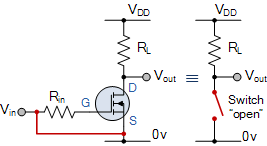
What is the mosfet: basics, working principle and applicationsCharacteristics of mosfet Mosfet as a switchMosfet circuits simple power testing transistors.
Analysis of mosfet as a switch with circuit diagram, exampleSchema und analyse eines common-source-mosfet-verstärkers High-power switching using mosfetsMosfet power characteristics indicated currents voltages fig where.
![[DIAGRAM] Circuit Diagram Of Jfet - MYDIAGRAM.ONLINE](https://i2.wp.com/electronicscoach.com/wp-content/uploads/2018/05/output-characteristics-of-jfet-circuit.jpg)
Mosfet drain characteristics circuit diagram
Mosfet inductive drivingMosfet drain characteristics circuit diagram Mosfet simple circuit diagram.
.


